Park FX Large Sample AFMs

Park FX Large Sample AFM Series is designed for high-precision and versatile surface characterization, ideal for both research and industrial settings. Supporting samples from small size up to 300 mm wafers, it is the ultimate solution for semiconductor manufacturing, materials research, quality assurance, and a range of other nanoscale applications including chemical analysis at nanoscale.

/content/dam/test/Appnote_img.jpg

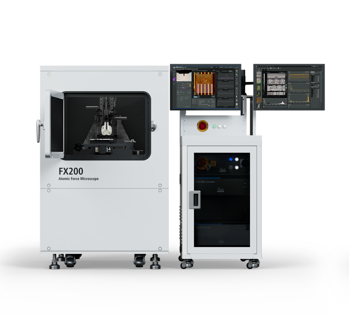
High-Precision & Versatile Performance

  •  Advanced mechanical structure ensuring minimal thermal drift and great stability
  •  Wide sample capacity supporting from small sizes to 300 mm wafers
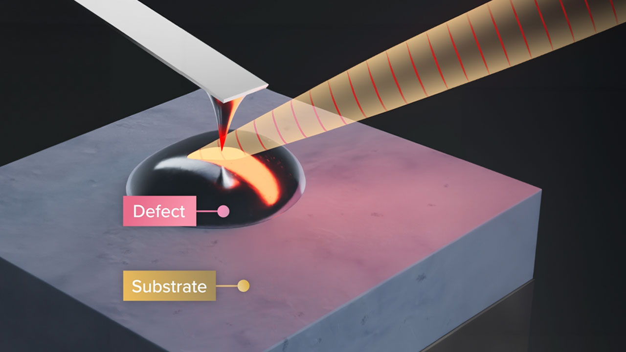
  •  Supports advanced nano-IR spectroscopy (PiFM) for precise chemical analysis
/content/dam/test/feature02.jpg

Simplified Workflow with Automated Features

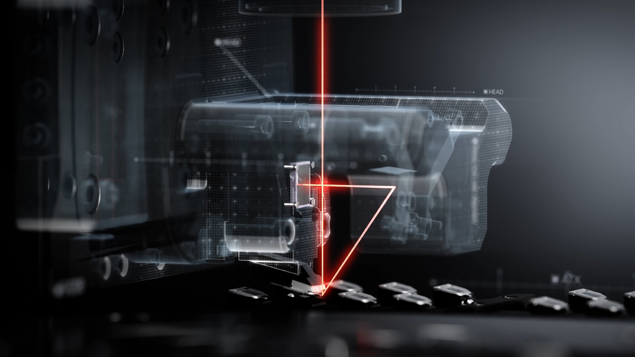
  • Automatic Probe Exchange with 16 probe slots enhancing efficiency with multiple experiments in one setup
  • Streamlines setup with automated tip mounting and laser beam alignment
  • StepScanᵀᴹ feature for automated sequential measurements at multiple coordinates
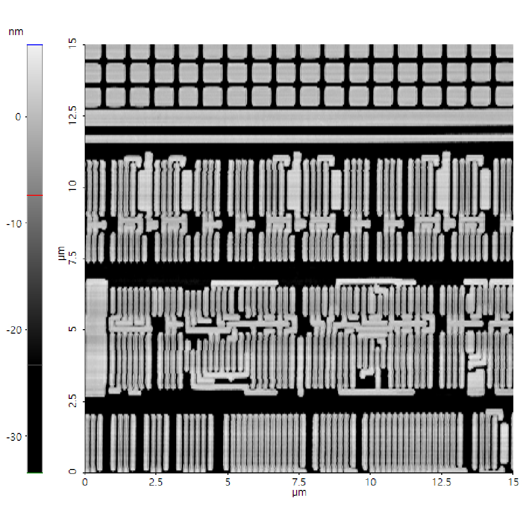
  • Macro optics for a large field of view (FOV), covering an entire 200 mm wafer sample
/content/dam/test/feature03.jpg

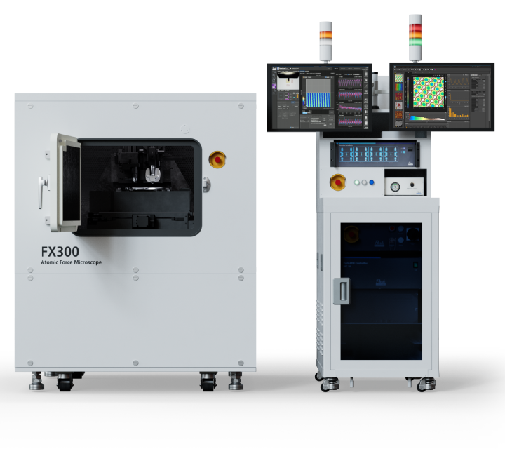
Specialized Features for Industrial AFM Applications

  • Specialized industrial R&D applications with long-range surface roughness profiling, recipe-based routine measurements and a rotatable stage
  • Improved sample visualization with optional advanced off-axis optical configurations
  • Integrated industrial-grade facility featuring a signal tower with an emergency-off unit, a facility controller, and optional contamination control solutions using a fan filter unit
FX40 with monitor

Park nano-IR Spectroscopy

Advanced Nanoscale IR Spectroscopy (PiFM) for Large Sample Chemical Analysis

Park NANO IR is an integrated infrared (IR) spectroscopy and atomic force microscopy (AFM) system. The spectroscopy part provides chemical identification under 10 nm spatial resolution. It uses a non-contact technique offering the safest spectroscopy scanning and the best in industry spatial resolution. The microscopy part provides nanometer 3D topography with sub-angstrom height accuracy and mechanical property information to the user.

Which Large Sample AFM is right for you?

FX200

FX200

The most advanced AFM for samples from small sizes up to 200 mm

FX300

FX300

Premier 300 mm AFM for Research, Quality Control, and Assurance

Sample Size
up to 200 mm
up to 300 mm
XY-Scan Range
100 µm x 100 µm
100 µm x 100 µm
Z-Scan Range
15 µm
15 µm
Multi-Sample
200 mm wafer sample chuck|holds up to 16 coupon-sized samples
300 mm wafer sample chuck|holds up to 16 coupon-sized samples
Auto Sample Setup
Yes
Yes
Auto Recipes
-
Yes
Rotation Stage
-
Yes
Chemical Identification Analysis
upgradeable
upgradeable

Designed for your Applications

Park FX Large Sample AFM provides precise measurements from the nanoscale to 300 mm wafers, making it the ideal solution in research and industry fields.

Semiconductor

Patterned Si Device

The structure of the device is evaluated using the non-contact mode. The image shows the width and depth of the patterned Si device.

Patterned Si Device

Semiconductor

Cu Pad

Cu pad image provides high-resolution analysis of surface roughness and structural features.

Cu Pad

Nanoelectrical Applications

Perovskite

AFM current image confirm the conductivity of the perovskite material. Current image reveals spatial variations in electrical properties.

Perovskite

2D materials

Moiré Superlattice in Twisted Bilayer Graphene on hBN

The two moiré patterns interfere, leading to a dual moiré superlattice. (Sample bias 0.05 V)

Moiré Superlattice in Twisted Bilayer Graphene on hBN

2D materials

Twisted bilayer graphene on hexagonal boron nitration

AFM current images of tBF/hbN shows the moiré patterns at nanoscale.

Twisted bilayer graphene on hexagonal boron nitration
FX40 with monitor

Unlock the FX200 Advantage

Discover how automated features are transforming AFM workflows

The FX200 is the latest large-sample Atomic Force Microscope (AFM) designed to enhance nanoscale surface analysis with advanced automation. This technical note provides a detailed overview of its key features, automation capabilities, improved sample navigation, StepScan technology, and experimental management system.