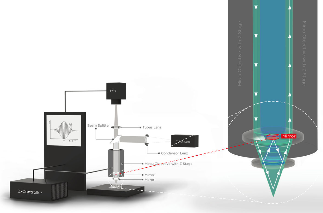
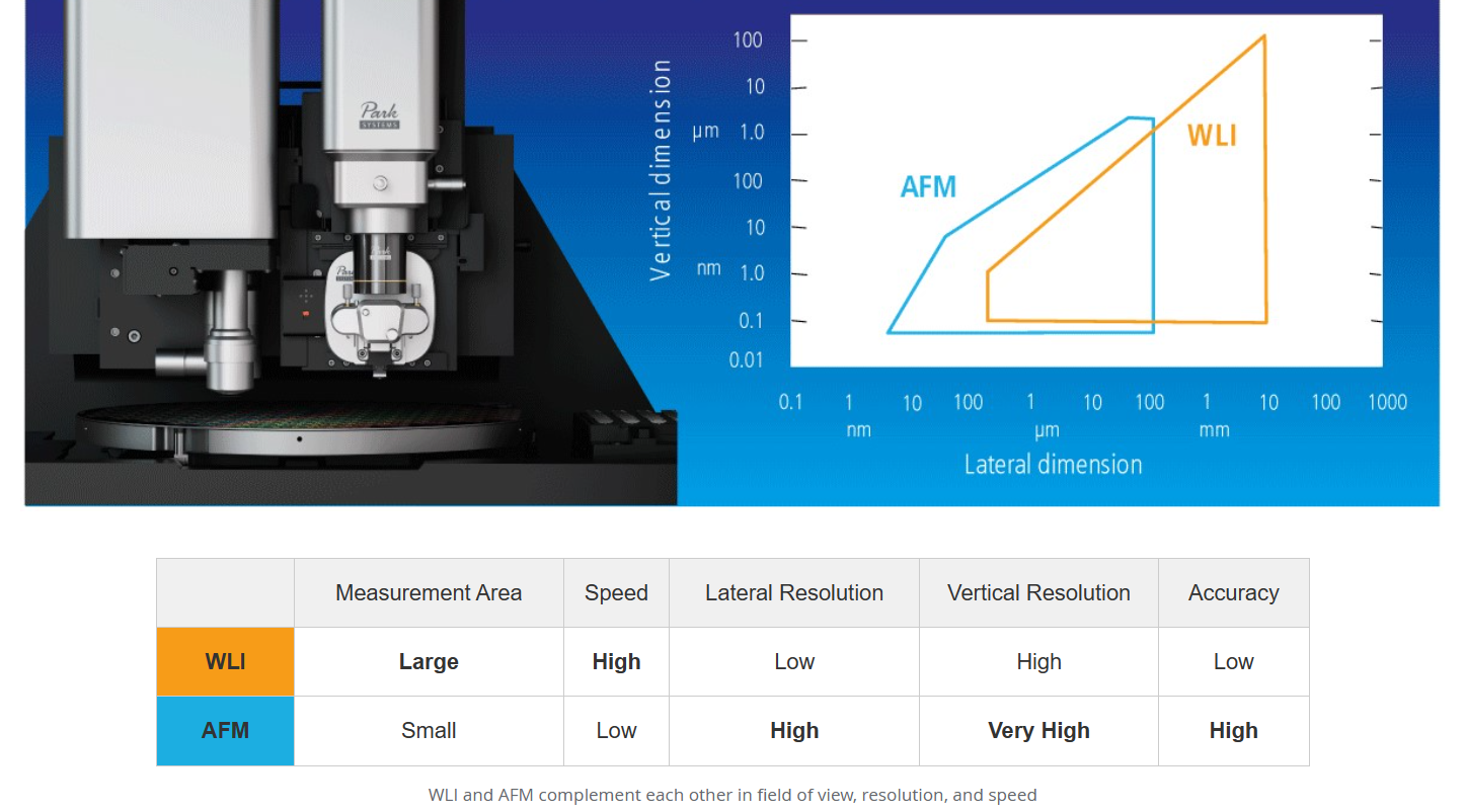
The AFM and White Light Interferometry(WLI) Technologies Built into One Seamless System
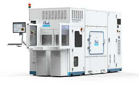
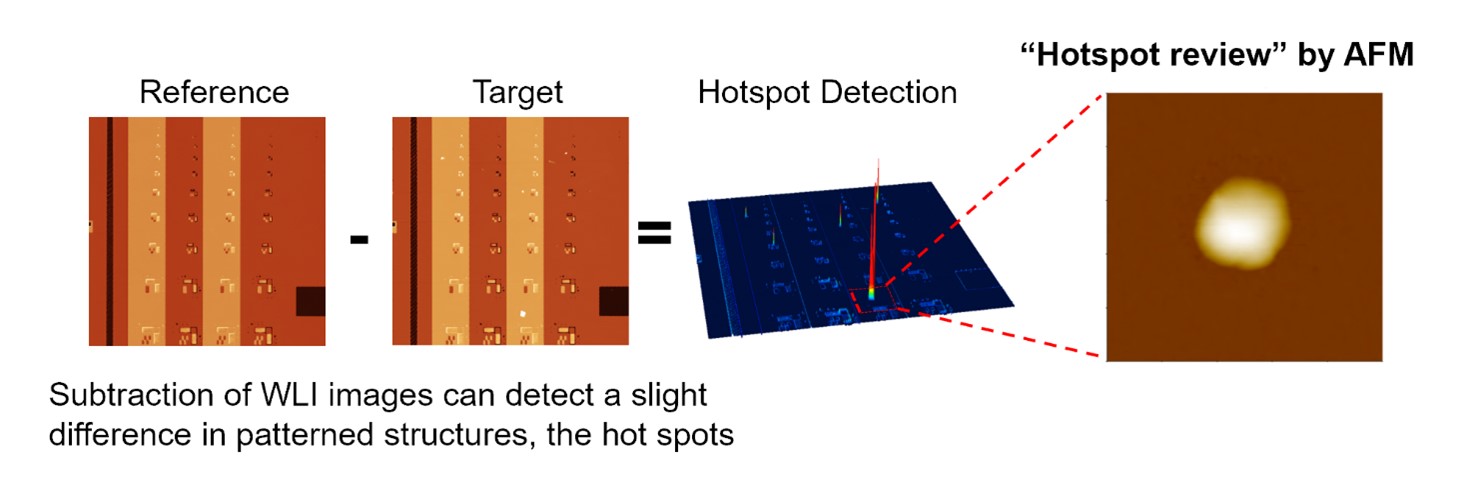
Park NX-Hybrid WLI is the first-ever AFM with built-in WLI profilometry for semiconductor and related manufacturing quality assurance, process control for semiconductor front-end, back-end up to advanced packaging, and R&D metrology. It is for those that require high throughput measurements over a large area that can zoom down to nanometer-scale regions with sub-nano resolution and ultra-high accuracy.


